The Wafer Foundry of SAW COMPONENTS offers you state-of-the-art technologies combined with 25 years of experience and a complete production made in Germany. We support you from the first development samples to mass production. In doing so, we place the highest value on quality, speed and flexibility.
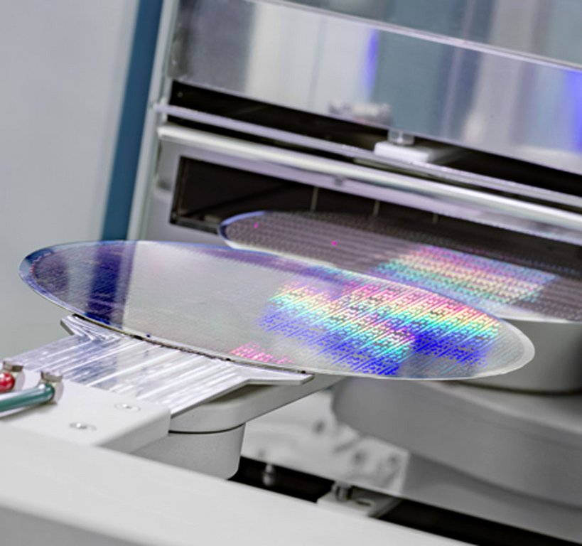
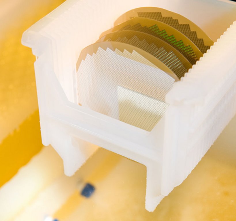
Wafer
- Wafer sizes: 100mm (4"), 150mm (6"), 200mm (8")
- Production on all common SAW or semiconductor substrates
- Quartz
- LiNbO3
- LiTaO3
- Bonded / POI wafers
- Glass / fused silica
- Langasite
- Silicon
- and others
- Polished on one and both sides
- other formats (thick or rectangular) possible
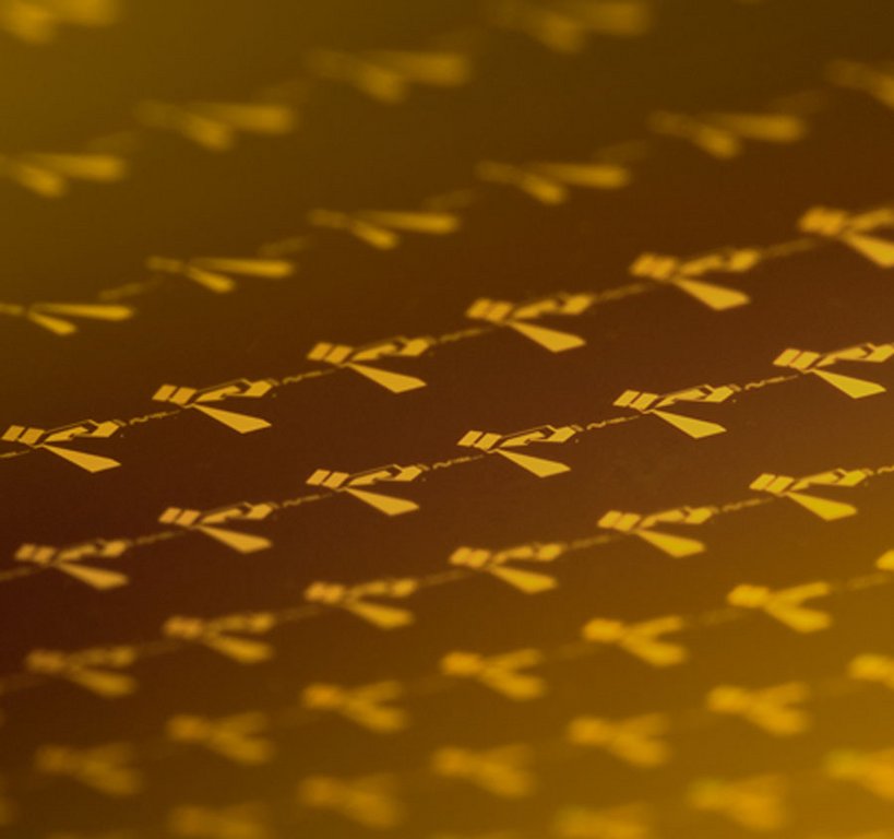
Lithography
- Processing of structure sizes up to 300nm
- high accuracy and yield
- Lift-off, wet etch or dry etch process
- I-line stepper lithography
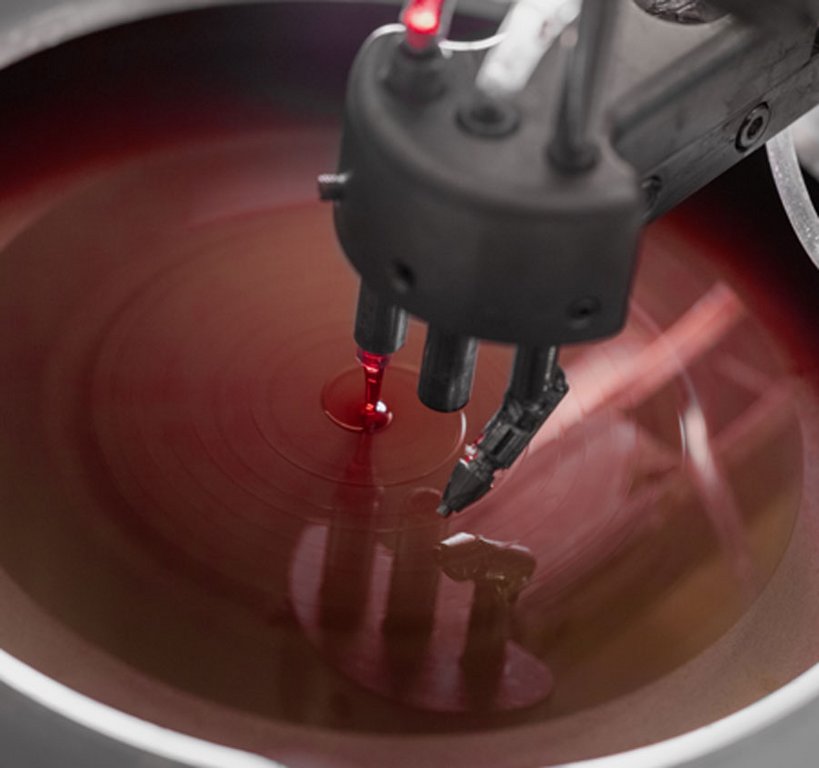
Thin-film technology
- Thin film technology with a precision of up to +/-10 nm with thicknesses from 1nm to 2500nm with all standard electrode materials (Al, Cu, Au, Ni, Pt, Ir, Zr, Pd, Ti, Cr and others) or their combination
- High Power coatings for use in the high power range
- 1-level or multi-level process
- Active Layer (IDT)
- Crossover layer with bridges
- Pad enhancement
- Passivation
- Under Bump Metallization (UBM)
- Backside metallization
Microfluidic and covering with Dry Film Resist
- multi-layer dry resist structures on the wafer
- for microfluidic systems and
- covering of cavities to protect active structures from contamination
- 10, 20, 90 µm layers
- 1-, 2- and 3-layer structures
- finest resolution by means of photolithography
- high durability and tested compatibility with wafer structures
Fast processing of your data
- Creation of masks with your customer data
- Digitization and processing of your mask data
- Data check before each tape out
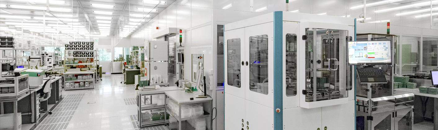
Clean Room
- 1000m² ISO 3 clean room (Class 10 Federal Standard)
Measurement and monitoring
We use various measuring devices to monitor and control processes and critical parameters:
- XRF for coating thickness measurement
- Probe section measuring device for layer thickness measurement on structured wafers
- AFM for surface and edge assessment
- Optical structure width measurement technology (i-line) down to 0.3µm (CD)
- Automatic wafer prober with NWA and HF probes
- Resistance measurement
- Ellipsometer for evaluation of semi-transparent layers
We carry out electrical wafer tests according to agreed tolerances and minimum yields (random sampling or 100% measurement):
- HF measurement
- s-parameter measurement
Production is located entirely in Germany and the company is completely independent. We place the highest value on the security and confidentiality of customer data and therefore work for customers all over the world.