We offer a wide range of assembly technologies for the correct packaging of your products. You can rely on proven complete solutions or use individual processes according to your requirements. Our production is certified according to ISO9001 and ISO13485 for medical devices. On request, we can perform individual qualifications and testing according to a wide range of standards.
Our packaging is specialized in:
- Clean Room ISO 6 (Class 1000 Federal Standard)
- Processing of special wafer materials such as silicon, glass, quartz, lithium tantalate, lithium niobate, etc.
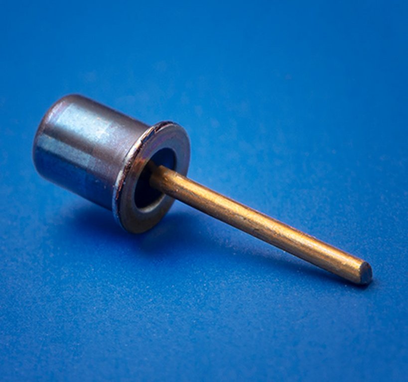
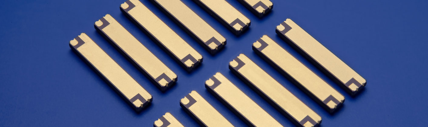
- Packaging of components in ceramic SMD and metal packages / DIP packages
- Packaging of bio-chips on circuit boards and medical cartridges (ISO 13485 medical product certified)
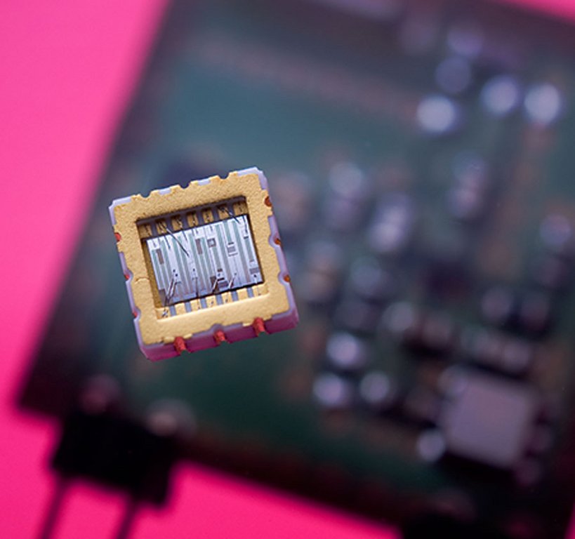
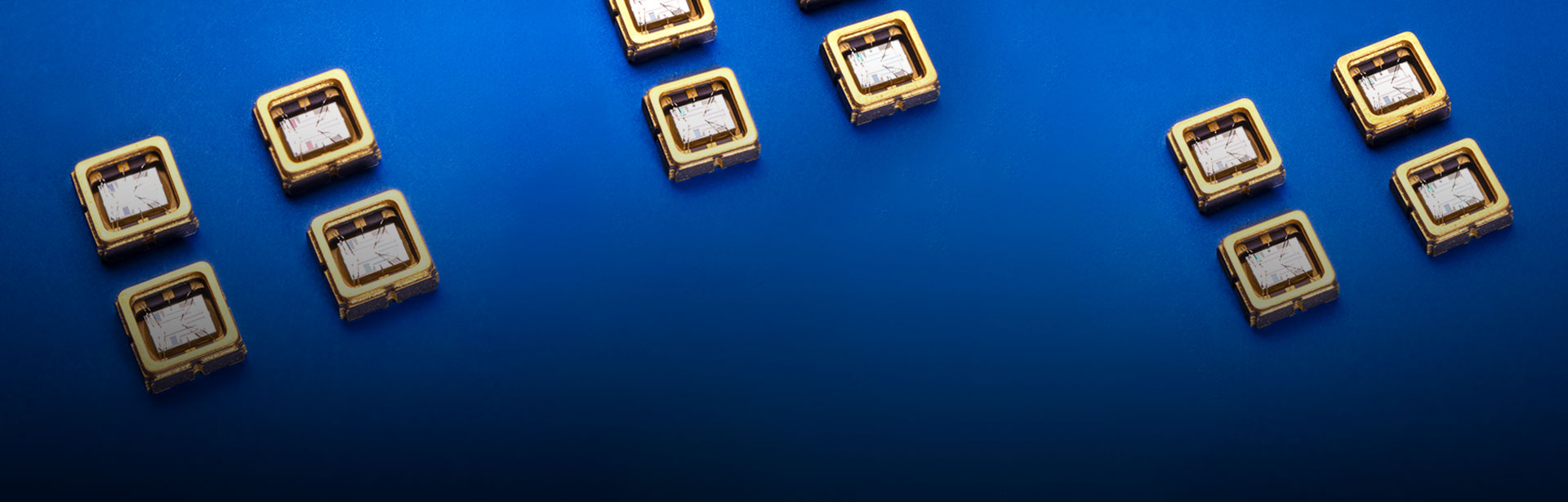
- Packaging of micro-optical components
- Packaging for harsh environmental conditions, e.g. for aerospace and defense applications
- Packaging for high operating temperatures up to 350°C
The available technologies include:
Chip assembly
- Plasma treatment with O2, Ar and other gases and mixtures
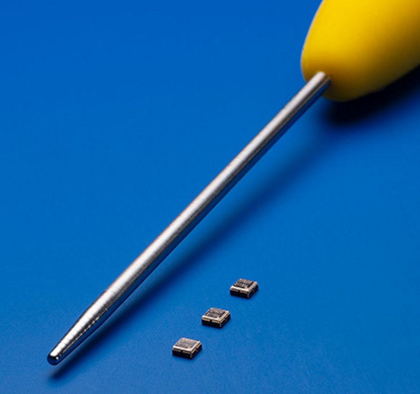
- Feeding of chips from wafers up to 200mm / 8"
- Automated package feeding
- Automated adhesive dispensing
Wire Bonding
- up to several thousand wires
- multi-level bonding
- AlSi wire 25µm
Capping
- Roll seam welding (Seam Welding)
- Welding of components with edge lengths of 2mm to 50mm
- Projection welding (Projection Welding)
- Sizes from 2mm to max. 36mm edge length, also round components (circumference max. 144mm)
- Tightness up to 10-9 mbar*l/s
- ealing takes place under inert gas atmosphere, e.g.
- N2 / He2 mixture
- Purified dry air
- Sealing under different gas atmospheres, mixtures of 3 different gases possible
- Fine leak tightness test
Laser processing
- Workpiece sizes of approx. 300mmx300mmx200mm can be processed
- Positioning and laser accuracy up to 25µm
- Markings of all kind
- Cutting of workpieces up to 500µm thickness